The DG8 RXtee Board for 28-432MHz

I designed this board because I needed a few compact bias-tee modules with built-in logic for remote switching of preamplifiers, transverters etc. Now that the design is working well, I’ve decided to make the board available in the GM3SEK Odd-Boards series for home constructors.
What’s a Bias Tee?
A “bias tee” is a simple way to feed DC power up the coax to remote devices such as preamplifiers and switching relays. At its very simplest, it consists of a series capacitor to pass the RF, and an RF choke to introduce the DC.

(To build a high power 1.8-50MHz bias tee, click here .)
- CAUTION: whenever you build a bias-tee, LABEL THE CONNECTORS!
Connecting a bias-tee the wrong way round can cause expensive damage because one of the two RF ports can deliver significant DC voltage and current into whatever equipment is connected. I have labeled the ports correctly above, and also on the PC board – “RF” and “RF+DC” – but the rest is up to you.
Features
The DG8 RXtee is several steps smarter than the basic bias tee above (although you can also wire it as a simple basic bias tee if that is all you need).
- Covers all RF frequencies from 28MHz to 432MHz (at least) with low loss and low VSWR (<1.05)
- Low-power applications only – not rated for handling high RF or DC power ( click here for details of a 1.8-50MHz high power version)
- DC supply typically 12-15V, currents up to ~1A with short-circuit protection
- Versatile TX/RX switching of the DC power (separate logic inputs for ground-to-transmit and TTL)
- Output for an external indicator LED
- Designed to fit inside a standard 20x20x37mm tinplate box (optional; user provides box and connectors – see parts list below).
- Supplied as a bare board only, for home constructors with sufficient experience to source the parts and assemble the board.
BOARDS NOW AVAILABLE – order here
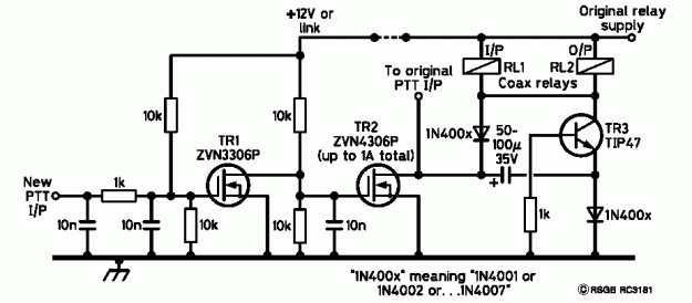
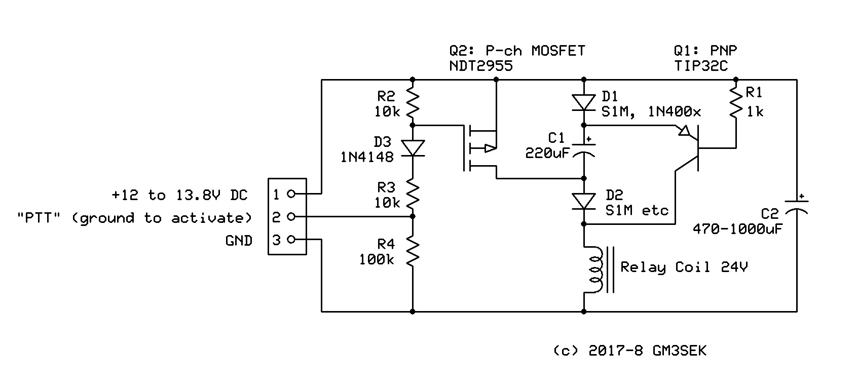
Schematic and Notes
 Click here to download as a printable .jpg file
Construction and connector options
You have choices! Get used to the idea of building things as you want them – not as someone else wants to sell them.
-
- As noted above, you can leave out the DC switching options if you don’t need them.
- This description features SMA female connectors soldered onto a screened tinplate box – a good general purpose option.
- If you wish, you can solder flying leads of RG174 or RG316 coax directly onto the box (or use a connector on one side, a flying lead on the other).
- If you don’t need screening, you can leave the box out completely and solder connectors and/or flying leads directly to the board.
Performance
All measurements were made on the prototype shown in the photographs, using the recommended Epcos 2.2uH RF choke.
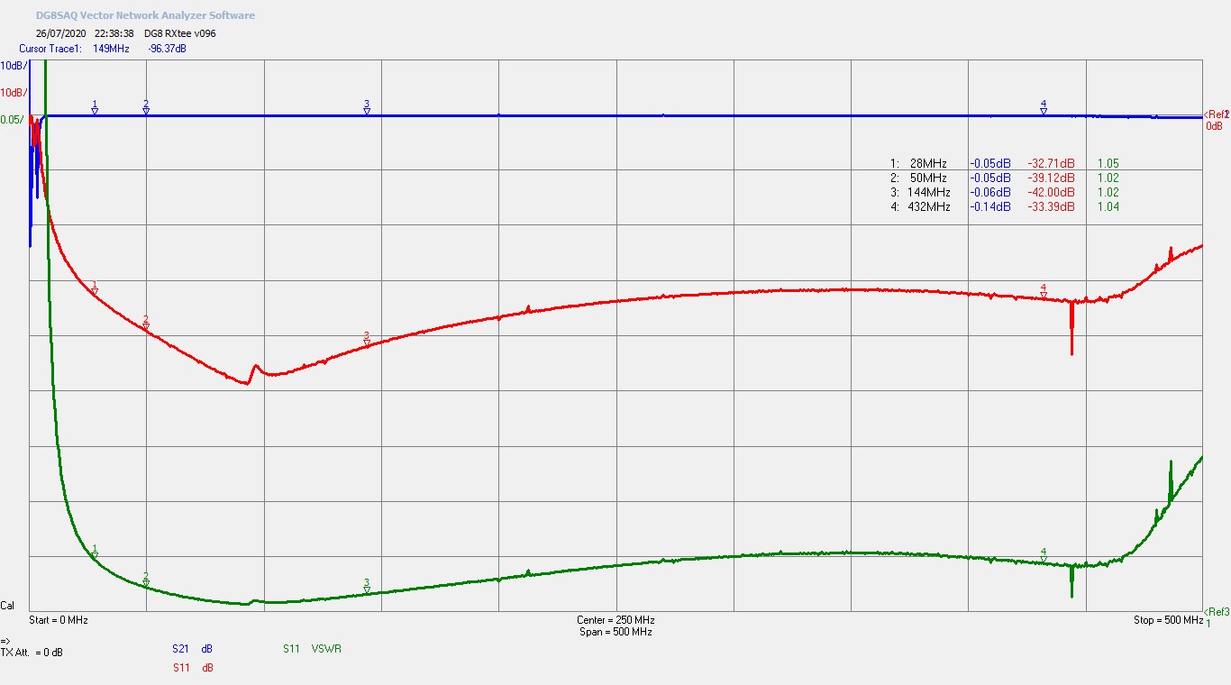
Click here to download as a printable .jpg file
Marker data from the above traces:
Freq Ins loss Rtn Loss VSWR
Marker 1 28MHz 0.05dB 33dB 1.05
Marker 2 50MHz 0.05dB 39dB 1.02
Marker 3 144MHz 0.06dB 42dB 1.02
Marker 4 432MHz 0.14dB 33dB 1.04
Parts List
C1, C5, C7: 100pF C0G dielectric, 0805 SMD (various sources)
C2, C4, C6, C9: 1nF (1000pF) C0G dielectric, 0805 SMD (various sources)
D1: 1N4148, 0805 SMD (various sources)
FB: Ferrite bead RF filter, 0805 SMD (various sources)
PTC: ‘Resettable Fuse’ rated to carry 1.0 A (various sources)
Q1: NDT2955, P-channel MOSFET, SMD (eg Farnell 9846271 )
Q2: 2N7002, TO-236AB SMD (eg Farnell 3439577 )
R1, R4: 10K, 0805 SMD (various sources)
R2: 220K, 0805 SMD (various sources)
R3: 1K0 0.25W, 1210 SMD (various sources)
RFC recommended: Epcos B78108S1222K000, 2.2uH 1A (eg Farnell 3806231 )
Optional:
RFC1, RFC2, C3 – 0805 pads are provided in case you need a 2-stage filter.
See notes on the Schematic above.
Tinplate box: Schubert type FG1, 20 x 20 x 37mm (un-punched) from G3NYK
External LED.
Construction Notes
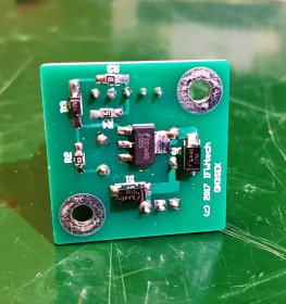
- For a high-resolution view of the completed DG8 RXtee, click here or click on the lead photo.
- For most applications you can use a single wire-ended RF choke, as shown in the prototype. If you really do need two-stage RF filtering, 0805 SMD pads are provided for RFC1, C3 and RFC2.
- If you are intending to mount the board in a tinplate box, see the detailed notes below. Your order of assembly must be as follows:
- file the board to be a snug fit inside the box with no gaps (board is supplied slightly over-width to allow this)
- check that the RF striplines end about 0.5-1.0mm away from the walls of the box.
- assemble the board and test the DC switching first (the underside of the board will be inaccessible when soldered into the box)
- install the RF choke last of all, after the board has been soldered inside the box.
- Here are close-ups of the top and bottom of the board with parts assembled ready for DC testing. (Later batches of the boards will have printed part numbers as shown on the right.)
Topside
C4 is soldered on top of C5; C6 is soldered on top of C7.


Underside


Installation in a tinplate box
Many small RF construction projects involve a PC board inside a tinplate shielding box, with accurately drilled holes for connectors. The detailed instructions below will be a useful checklist for other projects too.
1. Mark the box very carefully for drilling a pair of holes on opposite sides, as shown below (left, dimensions in mm)).

2. Accurately centre-punch the correct locations and then accurately drill a 1mm pilot hole in each side. Tip: this thin sheet steel isn’t easy to drill accurately. For the best possible start, use a short 1 x 3.2mm centre drill (eg Farnell 378756 ) to prevent the drill wandering off-centre.![]() 3. Check that the two holes are exactly opposite each other, square and level across the box, by feeding a 1.0mm drill through both holes. If all is well, use the same centre-drill to open out the holes to 3.2mm.
3. Check that the two holes are exactly opposite each other, square and level across the box, by feeding a 1.0mm drill through both holes. If all is well, use the same centre-drill to open out the holes to 3.2mm.
4. If necessary, line up the two holes using a round needle file. To avoid this horrible job, be careful and accurate when marking and drilling the pilot holes!
Tip: when drilling thin sheet metal, always clamp it down onto a piece of hardwood. (For this particular job, a scrap piece of 19mm floorboard fits nicely between the two sides of the box.)
5. If you are installing SMA connectors as shown above, open out the holes further to 4.0mm – again being careful not to go off-centre.
If you are installing flying leads of RG174 or RG316 coax, leave the holes at 3.2mm diameter.
6. Carefully de-burr the holes, inside and out.
7. Position the board accurately inside the box, and solder it into place. This is much easier If you are using SMA connectors that have a flat rear face. More detailed steps:
-
- Trim the PTFE insulation off the rear face and trim the remaining centre pin down to about 2.5mm. You should now find that the connector is self-locating inside its 4.0mm hole. Solder each connector into place, making sure the solder covers the entire rear of the flange (not easy to do neatly – see above).
- With the connectors in place, feed the pre-assembled and tested PC board into the box, underneath the connectors. Position the board straight and level within the box, with the two connector pins accurately centred along the RF striplines on the PC board.
Take your time to get this right.
Check that the ends of the RF striplines are not touching the side wall of the box! If in doubt, remove the board and use a sharp knife to chamfer the ends of the striplines (but don’t remove more than is really necessary). - Tack-solder the connector pins into place on both striplines. Check again that the board is level, and then tack-solder the far end of the board to the side wall of the box to hold it.
- Now seam-solder the PCB ground-plane to the wall of the box, at each side of each connector.
- Underneath the board, also seam-solder the accessible ends of the ground-plane as well.8. Install the RF choke as described above.
9. Find the other part of the box (it must be on the bench somewhere, right?) and trim one end to 8.0mm as shown above. This will leave room to connect wires to the row of pads on the board.
10. Last of all, assemble the whole box and test for correct operation.
As I said above, these “European tinplate box” techniques
will prove useful for a wide variety of small RF projects.
Page, circuit design and PC board,
all © 2020 IFWtech (Ian White, GM3SEK)